| Parameter | SITe | E2V | Units |
| Voltage noise | 8 | 20 | nV/sqrt(Hz) |
| 1/f corner freq | 10 | 150 | kHz |
| Gain | 1.5 | 4.5 | µV/e- |
| Output impedance | 2000 | 300 | ohms |
Preamplifier characteristics
| Parameter | OPA637 | Discrete | AD829 | AD8065 | Units |
| Voltage noise | 4.8 | 0.9 | 1.7 | 7.0 | nV/sqrt(Hz) |
| 1/f corner freq | 80 | 20 | 500 | Hz | |
| Current noise | .050 | .050 | 1.5 | 0.006 | pA/sqrt(Hz) |
| Settling time (0.1%) | 300 | 120 | 65 | 55 | ns |
| Gain-bandwidth | 80 | |
120 | 145 | MHz |
| Slew rate | 135 | 60 | 230 | 180 | V/µs |
For a typical CCD with a single-stage low-noise output amplifier, the minimum broadband voltage noise is about 6--8 nV/sqrt{Hz} with a 1/f corner frequency of 10 kHz. The output impedance of the on-chip amplifier can be as much as 2Kohms. A CCD with a dual-stage output may have an output impedance of around 300 ohms. The preamplifier noise should be substantially less than the CCD on-chip amplifier noise and have a lower noise corner frequency.
Monolithic FET input op-amps with acceptably low current noise and voltage noise exist, but only recent devices have fast enough settling times to operate at 2 µs per pixel or less. For example, the OPA637 op-amp (4.8 nV/sqrt{Hz}) takes more than 300 ns to settle to 0.1% and more than 450 ns to settle to 0.01% (of its final value). More recently, the AD8065 is now available with a slightly high voltage noise (7.0 nV/sqrt{Hz}) and settling time of 55 ns. During each pixel time, the preamplifer must settle once after reset (before the reference integration), and again after the charge is clocked to the output amplifier (before the signal integration). Long settling times either cut into the time available for integration, or they extend the pixel period.
Discrete component preamplifiers exist which are both fast-settling and low-noise, but these require a large number of parts and circuit board area. A typical design may have more than 50 separate components.
The preamplifier design we prefer has a matched JFET input buffer (SST404), followed by a low voltage-noise, fast-settling bipolar op-amp with high open loop gain (AD829). The circuit topology of each preamplifier is shown in the schematic. The overall preamplifier broadband noise is the rms sum of the JFET buffer voltage noise (1.5 nV/sqrt{Hz}), the op-amp input voltage noise (1.7 nV/sqrt{Hz}), and the op-amp input current noise (1.5pA/sqrt{Hz}) multiplied by the JFET output impedance. The JFET provides a low output impedance (300 ohms), so the op-amp input current noise contribution is small (0.6 nV/sqrt{Hz}). Overall, the preamplifier broadband noise is less than 3 nV/sqrt{Hz} (equivalent to less than 0.5 e- for 500 kHz bandwidth and 4.5 µV/e- CCD output node sensitivity).
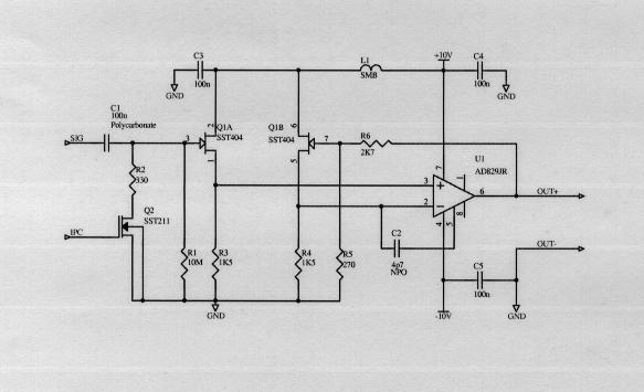
Preamplifier circuit (adapted from a design by J.Geary)
The CCD output amplifier load is a 10 kohm resistor, which is AC coupled to the low-noise, unity-gain JFET (SST404a) buffer, with a DC restore signal. The signal is amplified by a bipolar-input op-amp (AD829), with a gain of 10. The op-amp feedback loop features a matched JFET (SST404b) to balance the op-amp inputs, which minimizes the output offset voltage for zero input signal to the preamplifier. The preamplifier output is nominally 5 volts peak-peak at maximum signal. An associated ground reference is sent differentially with the preamp output signal to the signal processing circuits.
On the preamp circuit board, each trace which connects to the CCD has a series resistor plus a pulldown resistor to protect the device. The pulldown resistor ensures that each input is in a known state at power-up, or when the system is disassembled.
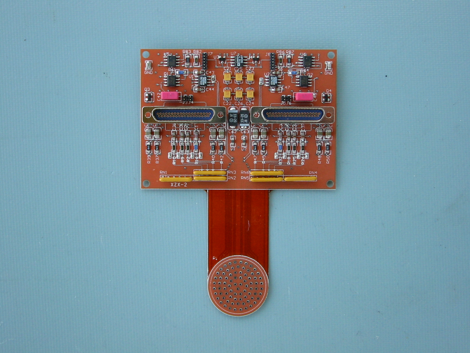
BASE preamplifier flex-circuit pcb
Greg Burley (burley@obs.carnegiescience.edu)
Ian Thompson (ian@obs.carnegiescience.edu)