Each signal processing channel features a well-known dual-slope integrator circuit topology, optimized in this case for fast-settling time.
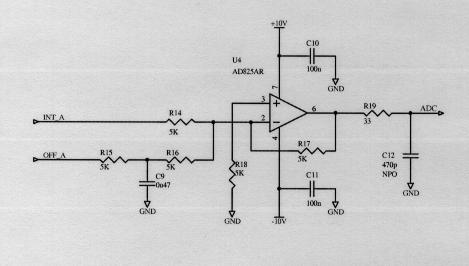
As shown in the schematic, the circuit configuration is that of a difference amplifier, followed by an op-amp integrator with complementary inputs. Analog switches select the input signal, reset the integrator capacitor and select one of the two gain settings. The integrator RC time constant is set by the selected resistor (either 2K or 5K), and a 560 pF capacitor. The integrator storage capacitor is a low leakage, temperature-stable polystyrene type. At the output of the integrator, the signal is buffered to provide a low-impedance source for the analog to digital converter, and a selectable voltage offset is introduced.
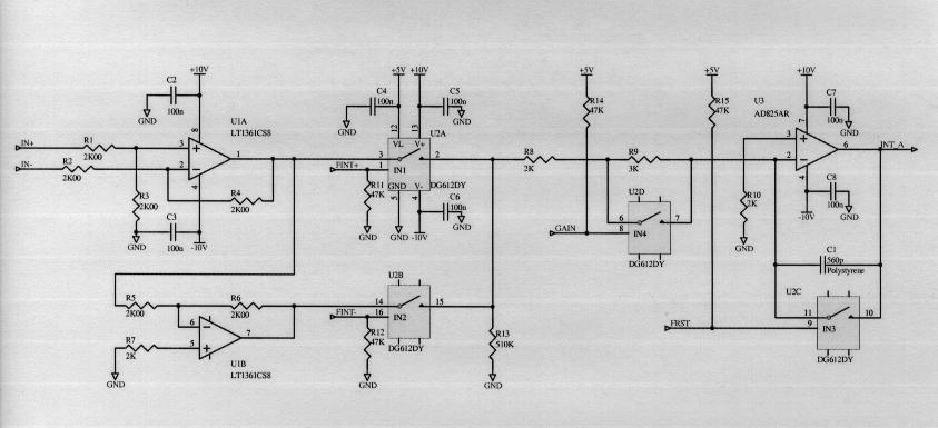
The op-amps of the dual-slope integrator signal chain were chosen for their low noise and fast settling times. A dual op-amp (LT1361) is used to maintain temperature tracking between the differential amplifier and the inverting amplifier. A FET input op-amp (AD825) is used for the dual-slope integrator for minimum bias and leakage current. The A/D converter is a hybrid 16-bit ADC4320B device from Analogic, with an internal sample-and-hold circuit. The sample-and-hold tracks the buffer op-amp output during the dual-slope integration and samples the stable signal at the end of the process. The data conversion is pipelined -- that is, the A/D conversion is started at the end of each pixel period with the result becoming available during the next pixel period. The maximum conversion time is 1.0 µs, which is adequate for a 500 kpixel/s readout rate (2 µs per pixel).
[ insert dual-slope waveform + control signals diagram]
Bias voltages
The ccd requires stable, low-noise bias voltages for its output transistor stages, and for the reset transistors (OD, OG, RD voltages). Each of these bias voltages is produced by a DAC output, followed by an op-amp gain stage (either G=5 or G=10). All bias voltages power up to zero volts.
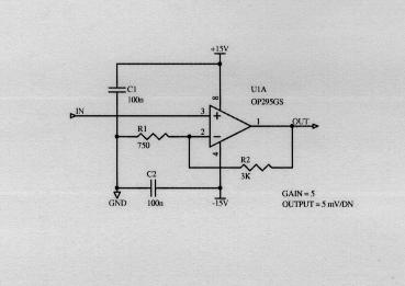
Typical bias voltage circuit
The output noise voltage of the DACs is fairly low (80 nV/sqrt(Hz)), but there is the possibility of crosstalk from the clock lines and power converters, so each bias voltage is low-pass filtered by an RC combination on the preamp board.
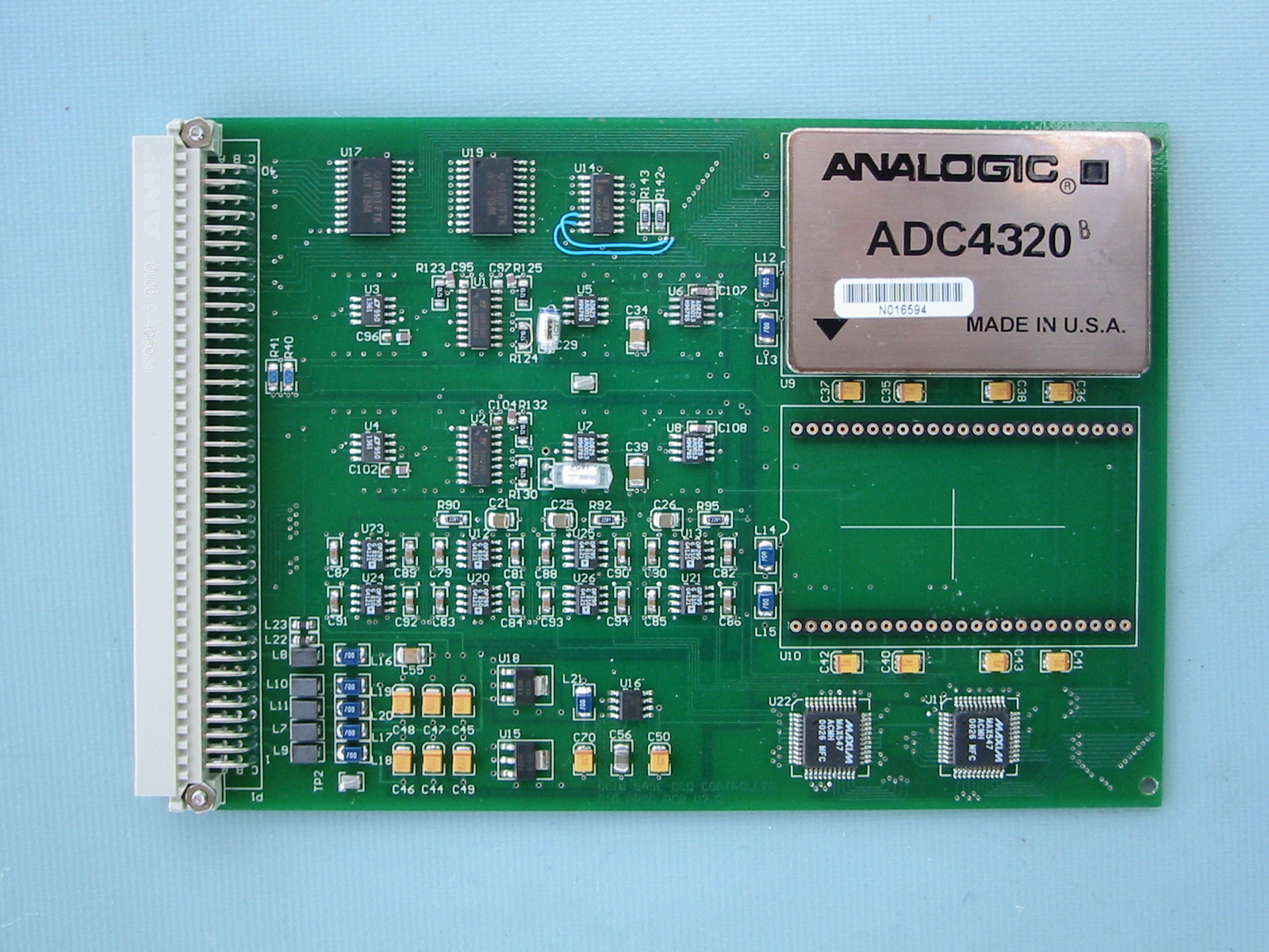
BASE signal processing pcb
Greg Burley (burley@obs.carnegiescience.edu)
Ian Thompson (ian@obs.carnegiescience.edu)