The optical link uses HP/Agilent LED transceiver modules and 62.5/100 µm glass multimode fiber. The data rate is 80 Mbps. Encoding and decoding of the data is performed in an Altera EPLD using a self synchronizing scrambler + descrambler pair.
Scrambling is used to get a DC-balanced output before transmission of the data over the optical link. Otherwise long strings of binary ones or zeros cause the average signal at the AC-coupled receiver to drift up and down. If the receiver input drifts to near the threshold value, any noise will cause bit errors.
In addtion, scrambling is quite useful for clock recovery. Long strongs of binary ones or zeros have no state transitions from which timing information can be extracted. By increasing the density of state transistions, it becomes much easier for the PLL at the receiving end to extract the clock signal from the data, lock onto the clock, and minimize jitter (and bit errors).
Several types of data coding are possible -- one can use an 8B/10B code (as per fiber channel, 1394b, gigabit ethernet), or a scrambler/descrambler (as per telcom long-haul optical systems).
From AT&T Bell Labs Transmission Systems for Communications [1] [2] [3] [4] -- a scrambler is a device which maps a digital sequence into a second sequence whose statistical properties are 'more random' in some sense. One simple form of scrambling consists of the addition of a pseudo-random sequence to the input data sequence. At the receiving end, descrambling is performed by subtraction of the same sequence.
![[1]](images/TransSysComm1.jpg)
![[2]](images/TransSysComm2.jpg)
![[3]](images/TransSysComm3.jpg)
![[4]](images/TransSysComm4.jpg)
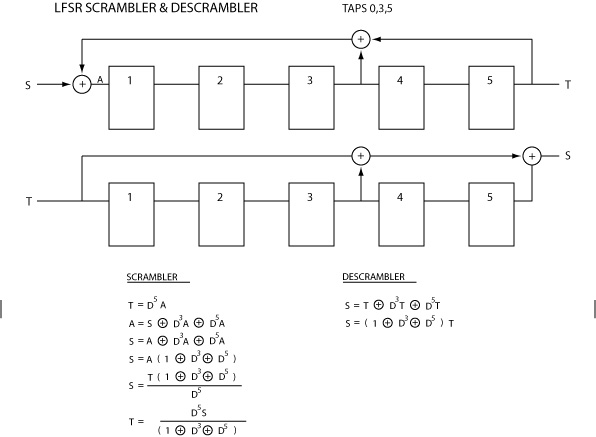
The pseudo-random sequence is generated by a linear feedback shift register (see diagram). The serial data enters the LFSR, where each stage is a D-type flip-flop equivalent to one time unit of delay. The delayed signal is tapped, with XOR (modulo-2) feedback with the input signal. For the descrambler, the XOR process is feed-forward.
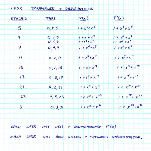
Linear feedback shift registers are often expressed in polynomial form. The table below lists the polynomial representations of a number of LFSRs. Certain combinations of taps are preferred to give maximal sequence length (see table).
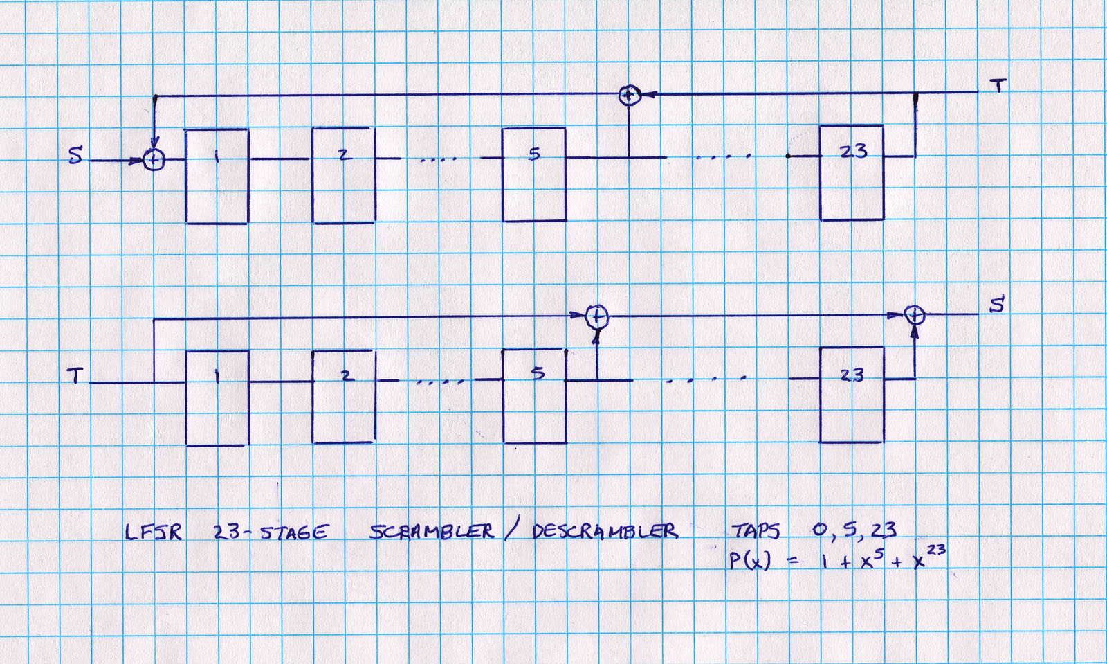
The previous diagram shows an n = 5 stage self-synchronizing scrambler/descrambler, implemented using LFSRs. For an n-bit LFSR, these will resynchronize after n bits if the scrambler and descrambler become desynchronized due to bit errors. A slight disadvantage is that each bit error is multiplied by the number of taps used by the LFSR (typically 3).
Some input data sequences to the LFSR can result in undesirable side effects. For instance, if the LFSR gets into an all-zero state, it will stay stuck in that state (so-called killer packet problem). The problem can be minimized by using a longer LFSR (say n>23), or adding logic to detect and correct the all-zeros state.
For most input sequences, the output of the scrambler will appear to be a random sequence of 1s and 0s, with a 0.5 probablility of each. That is, the output will be DC balanced. In addition, the output sequence will have a high density of transitions which are essential for clock recovery.

The figure shows the 'impulse response' of feeding a logic 1, followed by zeros to a 23-stage scrambler. After an initial delay of 23 clock cycles, the output (TXD) is randomized while the input (SDATA) is all zeros.
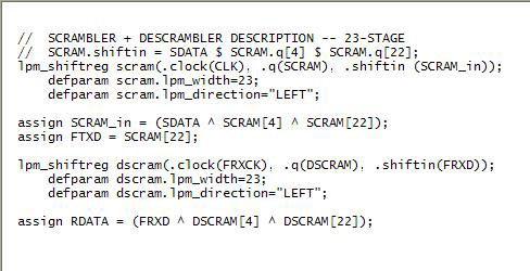
In EPLD terms, the following is the representation of a 23-stage scrambler/descrambler codes using Altera megafunctions in verilog. Note that the shift register numbering starts at 0, where the tap numbering for LFSRs normally starts at 1 (the reader can work out the correspondence).
Greg Burley (burley@obs.carnegiescience.edu)
Ian Thompson (ian@obs.carnegiescience.edu)