Clock drivers convert the logic level signals from the clock generator to the voltage levels required by the CCD.
The ccd requires separate clock drivers for each of the parallel clocks [IM3, IM2, IM1, ST3, ST2, ST1], and the serial clocks and reset gate [S3, S2, S1, RG].
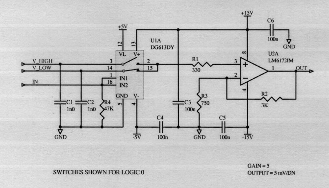
As shown in the schematic, the circuit topology is based on a fast analog switch (DG613), followed by an op-amp buffer. High and low output voltages (VH or VL) are set by a D/A converter. The analog switch output is either VH or VL depending on the input control sequence. The clock signals are amplified and buffered by high speed op-amps to drive the capacitive loads presented by the CCD.
Prototypes of this circuit indicate that switching times are approximately 25 ns. The rise/fall times of the clock signals are limited only by the slew rate and current output capability of the LM6172 op-amps. For typical on-chip parallel clock capacitance of 5 nF, the rise/fall times are 800 ns. For typical on-chip serial clock capacitance of 100 pF, the rise/fall times are 35 ns.
The analog switch chosen (DG613) features the best combination of fast switching time (20 ns ON, 15 ns OFF), and lowest charge injection (±2 pC) of available devices. Two drawbacks of the analog switch that require special attention are that it cannot operate from the full ±15 V supply voltages, and it requires 5V logic inputs (rather than 3.3V logic).
Clock drivers are provided for each of the control signals to the CCD, plus a few spares for future use. Separate DAC voltages are used for each parallel clock driver, the serial clock drivers, and the reset gate driver so that the voltage levels can be customized.
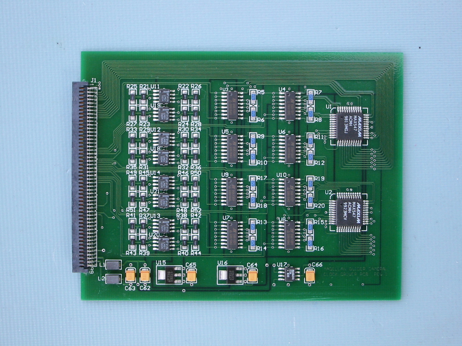
Guider camera clock driver board
Greg Burley (burley@obs.carnegiescience.edu)
Ian Thompson (ian@obs.carnegiescience.edu)