To perform an operation such as a serial or parallel shift the DSP steps though and writes the sequence of data words into an external 24-bit register via the DSP external bus [D0..D23]. Each sequence fragment is held in the external register until it is overwritten by the next fragment after a preset number of clock cycles, as coded into the DSP control software. The number of clock cycles (hold time) determines the timing of the clocks to the CCD. The time resolution of the clocking sequences is 25 ns. Program code and the clock sequence fragments are stored in the flash memory and loaded into the DSP on-chip memory during power up.
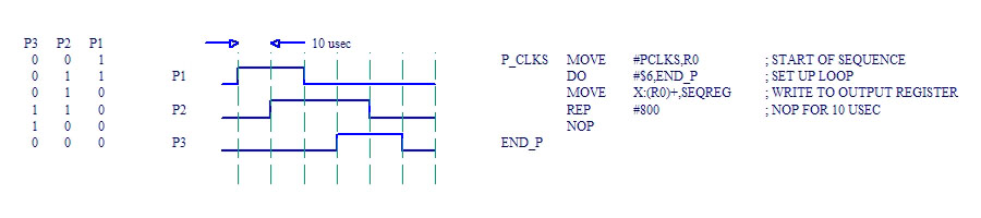
Each bit of the 24-bit DSP word represents one of the CCD control signals. With 24 bits, there are control signals for the image and storage area parallel clocks necessary for frame transfer [IM1-IM2-IM3, ST1-ST2-ST3] and the two sets of serial clocks necessary to use amplifiers at each end of the serial register [S1R-S2R-S3R-S1L-S2L-S3L-RG]. Other signals control the pixel conversion functions such as the dual slope integrator on/off and polarity, integrator capacitor reset, input clamp, and A/D converter start [FINT+, FINT-, FRST, IPC, /CONVST]. Spare bits allow additional signals to be added to accommodate different devices, as necessary.
Normally, for parallel transfers or frame transfer, the serial clocks and dual slope integrator control lines are held in a pre-specified state dictated by the CCD architecture. Similarly, the serial transfers require that the parallel clock lines be held in a specified state, possibly an MPP mode to reduce the dark current. This allows all control lines to be generated simultaneously as one 24-bit word.
A programmable logic device (EPLD) provides address decoding to allow the external clock register, and external analog-to-digital converter (ADC) and digital-to-analog converter (DAC) peripherals to be memory mapped. This simplifies the software a great deal by allowing each peripheral to be accessed as if it were a simple memory location. Each external peripheral has a dedicated chip select signal. During setup, the DSP writes to each individual DAC to set up the appropriate clock and bias voltages.
In addition, the PLD buffers the ADC data signals, reducing the possibility that high speed signals on the DSP data bus could corrupt the ADC conversion. The ADC signals connect to a quiet bus, and are bridged onto the DSP bus (by the PLD) only when each ADC is addressed.
Communication with a host computer is available via both a fast bi-directional serial link and a slower RS-232 monitor channel, using on-chip DSP peripherals. The DSP synchronous serial interface (SSI) transfers data via a bidirecitonal RS-644 (LVDS) or RS-485 link at up to 20 Mbps to/from a PCI interface, up to 100m away. The DSP serial communications interface (SCI) is a low speed RS-232 link to any generic computer serial port.
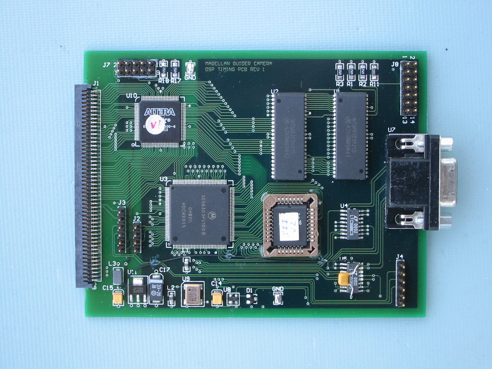
Guider camera DSP Timing pcb
Greg Burley (burley@obs.carnegiescience.edu)
Ian Thompson (ian@obs.carnegiescience.edu)